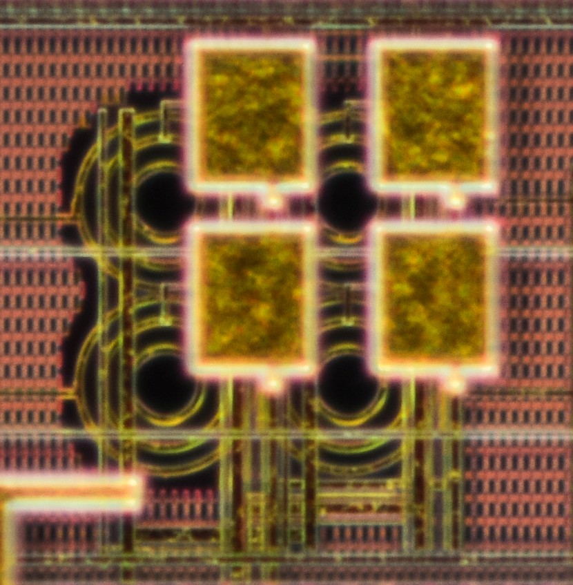
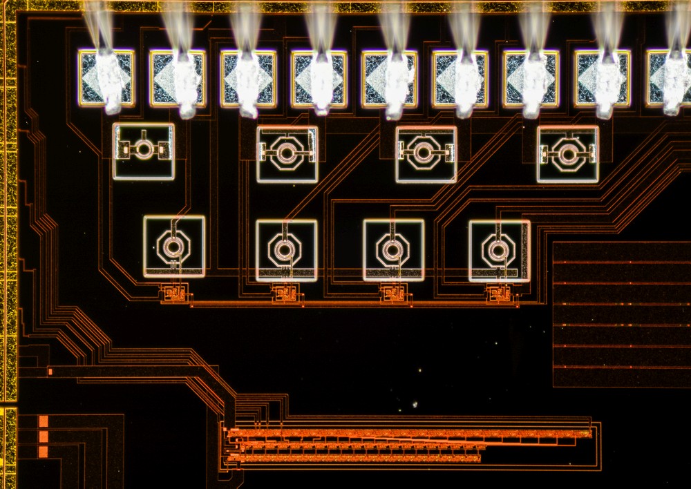
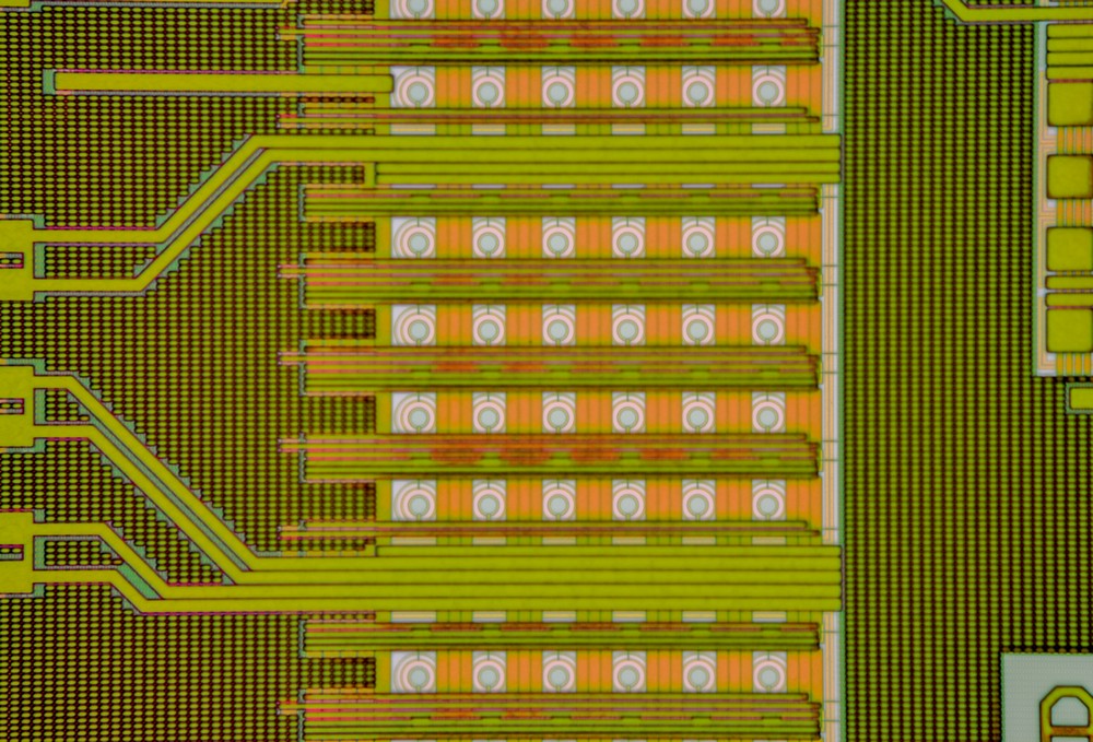
As early part of my doctorate studies at Oxford, I developed an analogue SPAD pixel which utilised the small gap between circular SPADs. The readout was compatible with conventional CMOS pixels. Digital SPAD pixels used a counter to store the number of detected photons. However, this counter occupied a large space relative to the diode. Instead the analogue pixel, stored the number of detected photons as a charge on the integrated metal capacitor which was placed above the quenching circuit. The stored charge was readout as an analogue voltage similar to CMOS pixel arrays.
D. Chitnis and S. Collins, "Compact readout circuits for SPAD arrays" , Proceedings of 2010 IEEE International Symposium on Circuits and Systems, pp.357-360, 2010
Danial Chitnis and Steve Collins, "A flexible compact readout circuit for SPAD arrays" , Proc. SPIE 7780, Detectors and Imaging Devices: Infrared, Focal Plane, Single Photon, 77801E (17 August 2010)
M. A. Al-Rawhani, D. Chitnis, J. Beeley, S. Collins and D. R. S. Cumming, "Design and Implementation of a Wireless Capsule Suitable for Autofluorescence Intensity Detection in Biological Tissues" , in IEEE Transactions on Biomedical Engineering, vol. 60, no. 1, pp. 55-62, Jan 2013


